-40%
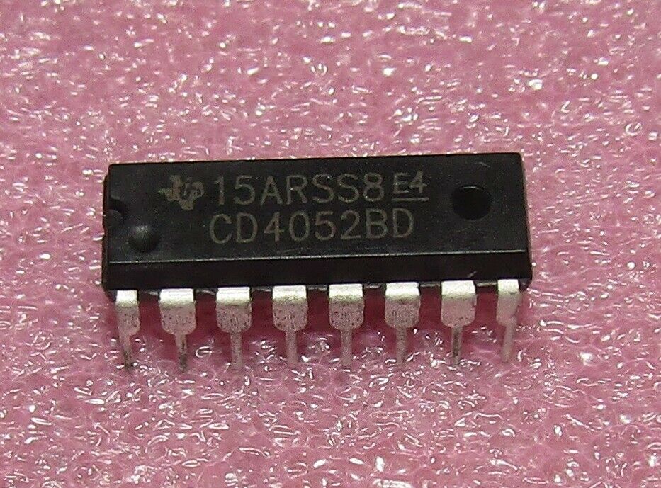
CD4052BD CD4052 CMOS Differential 4-Channel Analog Multiplexer/Demultiplexer
$ 2.9
- Description
- Size Guide
Description
CD4052BD CD4052 CMOS Differential 4-Channel Analog Multiplexer/Demultiplexer with Logic-Level ConversionBy TI
Description
The CD4052B are analog multiplexers are digitally-controlled analog switches having low ON impedance and very low OFF leakage current. Control of analog signals up to 20V
P-P
can be achieved by digital signal amplitudes of 4.5V to 20V (if V
DD
–V
SS
= 3V, a V
DD
–V
EE
of up to 13V can be controlled; for V
DD
–V
EE
level differences above 13V, a V
DD
–V
SS
of at least 4.5V is required). For example, if V
DD
= +4.5V, V
SS
= 0V, and V
EE
= –13.5V, analog signals from –13.5V to +4.5V can be controlled by digital inputs of 0V to 5V. These multiplexer circuits dissipate extremely low quiescent power over the full V
DD
–V
SS
and V
DD
–V
EE
supply-voltage ranges, independent of the logic state of the control signals. When a logic "1" is present at the inhibit input terminal, all channels are off.
The CD4052B is a differential 4-Channel multiplexer having two binary control inputs, A and B, and an inhibit input. The two binary input signals select 1 of 4 pairs of channels to be turned on and connect the analog inputs to the outputs.
When these devices are used as demultiplexers, the "CHANNEL IN/OUT" terminals are the outputs and the "COMMON OUT/IN" terminals are the inputs.
Features
Wide Range of Digital and Analog Signal Levels - Digital...3V to 20V - Analog..≤ 20V
P-P
Low ON Resistance, 125R(Typ) Over 15V
P-P
Signal Input Range for V
DD
–V
EE
= 18V
High OFF Resistance, Channel Leakage of ±100pA (Typ) at V
DD
–V
EE
= 18V
Logic-Level Conversion for Digital Addressing Signals of 3V to 20V (V
DD
–V
SS
= 3V to 20V) to Switch Analog Signals to 20V
P-P
(V
DD
–V
EE
= 20V)
Matched Switch Characteristics, r
ON
= 5R (Typ) for V
DD
–V
EE
= 15V
Very Low Quiescent Power Dissipation Under All Digital-Control Input and Supply Conditions, 0.2µW (Typ) at V
DD
–V
SS
= V
DD
–V
EE
= 10V
Binary Address Decoding on Chip
5V, 10V and 15V Parametric Ratings
10% Tested for Quiescent Current at 20V
Maximum Input Current of 1µA at 18V Over Full Package Temperature Range, 100nA at 18V and 25°C
Break-Before-Make Switching Eliminates Channel Overlap
Applications
Analog and Digital Multiplexing and Demultiplexing
A/D and D/A Conversion
Signal Gating
TERMS OF SALE
We welcome FPO/APO/Military Orders.
APO/FPO ships at domestic rates.
New Bidders, International bidders welcome - we are flexible on customs declarations.
Any questions eoi at lunaticlabs.biz
WINDHAGBATS


